Whenever you begin an STM32 MCU with its default configuration, its CPU will tick alongside at a leisurely variety of cycles on the order of 8 to 16 MHz, utilizing the high-speed inner (HSI) clock supply as a secure default to bootstrap from. After this section, we’re free to go wild with the system clock, in addition to the varied clock sources which can be out there past the HSI.
Growing the system clock doesn’t simply have an effect on the CPU both, but additionally impacts the MCU’s inner buses through its prescalers and with it the peripherals like timers on that bus. Therefore it’s important to know the clock material of the goal MCU. This text will deal with the final case of accelerating the system clock on an STM32F103 MCU from the default to the utmost rated clock velocity utilizing the related registers, bearing in mind elements like Flash wait states and the APB and AHB prescalers.
Though the Dhrystone benchmark is moderately old style now, it’ll be used to display the distinction {that a} sooner CPU makes, in addition to how complicated precisely benchmarking is. Plus it’s simply attention-grabbing to get an thought of how a lowly Cortex-M3 based mostly MCU compares to a as soon as top-of-the line Intel Pentium 90 CPU.
Stitching The Clock Material
The F103’s clock tree isn’t an identical to that of different households of STM32 MCUs, however the fundamental ideas stay the identical. See the under graphic from Reference Guide 0008 for the clock tree of STM32F10x MCUs:
We will see the HSI clocked at 8 MHz, which feeds into the clock enter swap (SW), from the place it might present the 8 MHz system clock with out additional fuss. Our different choices are to make use of the HSE, which is fed in through its respective oscillator pins and from there’s wired to the identical swap because the HSI. If we wish to get the next clock velocity than what the HSI or HSE can present instantly, we have to use the Section Locked Loop (PLL) to generate the next clock velocity.
For this we have to first configure the PLL, allow it and choose it because the enter supply for the clock swap. Earlier than we will throw the swap, nonetheless, we additionally have to ensure that the prescalers for the buses (APB1, APB2, AHB) are set accurately. As we will see within the clock tree diagram, now we have most speeds for every bus and stuck scaling numbers for every prescaler.
This sample continues with particular person peripherals, a few of which even have their very own prescaler – like USB and the ADC – however that is simply one thing to bear in mind for when utilizing these peripherals. If we’re simply making an attempt to crank the CPU core as much as its most velocity and nonetheless wish to use the UART, all we want is to get the PLL configuration proper, together with the AHB and APB prescalers in order that the UART peripheral might be interacted with.
Plugging In Numbers
Earlier than we begin fortunately punching numbers on our keyboard to make the MCU go sooner, there’s one tedious element that now we have maintain first: appeasing the Flash reminiscence in order that it might sustain. This entails configuring the best variety of wait states, the usage of prefetching and related choices. For this we open our copy of RM0008 to web page 60 to ogle on the FLASH_ACR register and its choices.
On this Flash entry management register for the F103 and kin we get to allow or disable the prefetch buffer and the latency. Thankfully, for the latency the RM tells us precisely what number of wait states now we have to set right here relying on our goal system clock velocity. For the 72 MHz that the F103 is rated for, now we have to set two wait states.
Scrolling up a bit to web page 58 and doing the unspeakable factor of studying the documentation, we will see that the prefetch buffer is turned on after reset by default and is greatest left enabled. As for the half cycle possibility, that is associated to ‘energy optimization’, which signifies that you’ll not contact this except you realize what you’re doing and are certain that that you must change this.
Consequently we will configure our Flash as:
FLASH->ACR |= 2 << FLASH_ACR_LATENCY_Pos | FLASH_ACR_PRFTBE;
Subsequent we want to use the HSE through the PLL to get probably the most correct and quickest system clock velocity, which first requires allow the HSE and ready for RCC_CR_HSERDY to vary to 1 as point out that it’s prepared to be used.
RCC->CR & RCC_CR_HSEON
whereas ((RCC->CR & RCC_CR_HSERDY) == 0) {
    // Deal with time-out.
}
Up subsequent is configuring the PLL, beginning with setting the PLL supply to HSE:
RCC->CFGR |= RCC_CFGR_PLLSRC;
Now we will configure the AHB and APB prescalers. These take the brand new system clock and divide it by the set quantity. For the F103, the 36 MHz-limited APB1 must be set to 2, whereas AHB and APB2 can run on the full 72 MHz, ergo 1.
RCC->CFGR |= 1 << RCC_CFGR_HPRE_Pos;
RCC->CFGR |= 2 << RCC_CFGR_PPRE1_Pos;
RCC->CFGR |= 1 << RCC_CFGR_PPRE2_Pos;
Last Steps
Persevering with configuring of the PLL and assuming that it’s at the moment disabled, we will now mash in its multiplier quantity. Not like different STM32 households, the F1’s PLL is moderately easy, with only a single multiplication issue. Since we’re utilizing the HSE, we have to know the board that we’re utilizing and the velocity that this HSE oscillates at. Taking the frequent ‘Blue Tablet’ STM32F103 board as instance, this options an 8 MHz HSE enter, which means that now we have to multiply this by 9 to get the goal of 72 MHz.
RCC->CFGR |= 7 << RCC_CFGR_PLLMULL_Pos;
The goal PLLMUL register begins at 0x02 for a multiplier of x4, ergo we have to subtract two from our goal multiplier. With that performed we will allow the PLL and look ahead to it to stabilize:
RCC->CR |= RCC_CR_PLLON;
whereas (!(RCC->CR & RCC_CR_PLLRDY)) {
    // Timeout dealing with.
}
Subsequent we throw the large swap to make use of the PLL’s output because the system clock supply and look ahead to the swap to finish:
RCC->CFGR &= ~(RCC_CFGR_SW);
RCC->CFGR |= RCC_CFGR_SW_PLL;
whereas (!(RCC->CFGR & RCC_CFGR_SWS_PLL)) { }
We must be up and operating now, leaving us simply to replace the worldwide CMSIS SystemCoreClock variable with the brand new clock velocity of 72 MHz.
Benchmarking
Operating Dhrystone on our F103 looks like a little bit of a problem because the benchmark was created to your typical desktop and server methods. To attain this, I took the unique pre-ANSI C code for Dhrystone 2.1 and tailored it to a Nodate challenge. The dhrystone.cpp file accommodates the benchmark itself, with no vital modifications aside from to arrange the MCU and the UART as customary output goal. The variety of runs can be hardcoded to be 100 million in order that it doesn’t must be punched in each time.
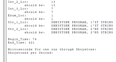
After compiling the benchmark and flashing it to the STM32F103 board, it appeared to take a couple of eternities for it to finish with so many runs. When the board’s single LED lastly began doing its leisurely blinking routine to point completion, it turned out that 347 seconds had expired, or roughly 5.78 minutes. As might be seen within the begin time, this wasn’t the primary try, after a ten million run accomplished too rapidly in keeping with the benchmark’s standards. C’est la vie.
Annoyingly, the printf-lite implementation that I take advantage of with Nodate didn’t appear to love the 32-bit float values and have been absent within the ultimate output, so I needed to do the calculations for the Dhrystones Per Second (DPS) and associated MIPS (DPS / 1757) myself. Because the instances() implementation’s ticks equal seconds, this was at the least pretty simply, giving the next numbers:
- DPS: ~288,184.438
- MIPS: ~164.021
To see whether or not these numbers are in any respect believable, I consulted a couple of lists of Dhrystone benchmark outcomes, together with one for DPS and one for MIPS. Making an allowance for the noise created by operating it on an OS versus naked steel, my use of -Og optimization degree and different variations, the location on the degree of a few Pentium 100 doesn’t appear too farfetched.
There’s an official ARM Dhrystone benchmarking information (AN273), which cites a DPS of 40,600.9 for a Cortex-M MCU operating at 18.5 MHz. This might be 158,014 DPS if extrapolated linearly, however clearly not the precise board, MCU or compile flags are used, so ‘tough ballpark’ appears to be the time period of the day right here.
Maybe probably the most attention-grabbing discovering is {that a} lowly STM32F103 MCU can sustain with a as soon as high-end Pentium CPU of the early Nineties, at the least throughout the restricted integer-only Dhrystone benchmark. Subsequent goal will most likely be to run the extra fashionable and in depth CoreMark on the F103 and different STM32 MCUs, to provide a extra holistic perspective.


